I always wanted to understand how a CPU works, how it transitions from one instruction to the next and makes a computer work. So after reading Ken Shirrif’s blog about a bug fix in the 8086 processor I thought: Well, let’s try to write one in a hardware description language. This post is a write up of my learning experiment.
I’ll walk through my steps of creating an emulator, compiling and linking C for bare metal, CPU design and finally the implementation of my toy RISC-V CPU.
Goals
- implement a CPU in a hardware description language (HDL),
- code must be synthesizable (except memory),
- simulate it,
- and run a bare metal C program on it.
While I had plenty research time, I had only about 30 hours of development time. Without prior hardware design experience the goals had to be simple enough:
- RISC V Integer instruction set only (minus system and break calls),
- no interrupt handling or other complexities,
- no or only minimal optimizations.
My test program written in C is Conway’s game of life, try the interactive web version.
In a future iteration I plan to run my project on a real FPGA and implement a memory controller. Let’s say I made it to about 85% of what I wanted to achieve.
Write an emulator
Writing an emulator, i.e. a program that can execute the instructions of a CPU, is an excellent stepping stone towards a hardware implementation. For me - without a hardware background - it is much easier to reason about and learn the instruction set.
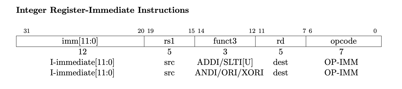
So my first step was to understand the RISC V instruction set. The RISC V specification is quite long, but I only needed chapters 2 (integer instruction set), 19 (RV32 / 64G instruction set listings) and 20 (assembly programmer’s handbook). These give detailed definitions of how each instruction must be executed, what kind of registers must be implemented, etc.
Let’s look at an example: Arithmetic / logical instructions operating on a register and an immediate value. For ADDI (add immediate) the following is done: rd <- rs1 + imm: The register identified by rd is set to the sum of the value stored in register rs1 and the value given in the instruction itself.
The emulator is implemented in C++ with a C-style interface in a shared library. This makes it easy to hook it into Python via cffi. This saved me quite a bit of time for file system and user interactions, which were all done in Python.
struct RV32EmuState;

extern "C" RV32EmuState* rv32emu_init();
extern "C" void rv32emu_free(RV32EmuState *state);

extern "C" void rv32emu_set_rom(RV32EmuState *state, void *data, uint32_t size);
extern "C" void rv32emu_read(RV32EmuState *state, uint32_t addr, uint32_t size, void *p);

extern "C" int32_t rv32emu_step(RV32EmuState *state);
extern "C" int32_t rv32emu_run(RV32EmuState *state, uint32_t *breakpoints, uint32_t num_breakpoints);

extern "C" void rv32emu_print(RV32EmuState *state);
The core of the emulator is the rv32emu_step function, which executes exactly one instruction and then returns. In RISC V each instruction is exactly 32 bits. It first decodes the op code (what kind of operation) and then the specific operation (e.g. ADD immediate). It’s a large, nested switch.
int32_t rv32emu_step(RV32EmuState *state) {
    uint32_t *instr_p = (uint32_t*)(_get_pointer(state, state->pc));
    uint32_t instr = *instr_p;

    // decode
    uint32_t opcode = instr & 0x7F; // instr[6..0]

    switch(opcode) {
        //
        // ... all opcode types ...
        //
        case OPCODE_OP_IMM: {
            uint32_t funct3 = (instr >> 12) & 0x07; // instr[14..12]
            uint32_t rs1 = ((instr >> 15) & 0x1F);

            uint32_t imm = (instr >> 20) & 0x0FFF; // 12 bits
            uint32_t imm_sign = instr & (1ul << 31);
            if(imm_sign) {
                imm |= 0xFFFFF000;
            }

            uint32_t data1 = state->reg[rs1];
            uint32_t data2 = imm;
            uint32_t reg_dest = (instr >> 7) & 0x1F;
            if(reg_dest != 0) { // register 0 is always zero and never written too
                switch(funct3) {
                    //
                    // ... all OP_IMM instructions ...
                    //
                    case FUNCT3_OP_ADD: {
                        state->reg[reg_dest] = data1 + data2;
                        break;
                    }
                }
            }
            break;
        }

    // ...

    state->pc += 4; // go to next instruction for non-jump / non-branch
    return 0;
}
The mathematical and logical operations are simplest to implement, so I started with them. Iteratively I’ve added branches, jumps and the remaining logic until I had covered all instructions other than ECALL and EBREAK. These two were not necessary for my bare metal experiment.
For testing I relied on simple hand-written assembly code. Of course this did not exercise my emulator thoroughly. So as a next step I wanted to finally run my Conway’s game of life simulation.
Cross compiling, linking and ELF to bin
Going from C to a bare metal CPU takes a few steps: cross compile, ensure proper memory layout and converting the ELF file to a binary blob. Also instead of having a main function my code has a _start function defined as follows:
void __attribute__((section (".text.boot"))) _start() {
    run(); // call the actual "entrypoint"
}
I’ll explain the details later.
My CPU only supports the RISC-V 32 bit integer instruction set, but my host system is running on x86-64. So I needed a cross compiler and used the Ubuntu package gcc-riscv64-unknown-elf. Then I could compile my code using the following command:
riscv64-unknown-elf-gcc -march=rv32i -mabi=ilp32 \
    -nostdlib -ffreestanding -Tprograms/memory_map.ld \
    -o life.rv32.elf life.c
Let’s take this apart:
- execute the RISC-V cross-compiler
- set it’s architecture to rv32i, which is RISC-V 32bit integer instruction set
- define the application binary interface, i.e. conventions how to emit assembly. This makes it so that integers, longs and pointers are 32 bit
- these three are needed to emit code compatible with my emulator and later CPU
- compile without a standard library
- Standard libraries like the system libc assume operating system support, but my toy CPU will be running bare metal. So we have to switch that off. This means we won’t have access to
malloc,printf,putsetc. Instead we’ll need to implement this ourselves, if we want to use it. This means we have no startup code either.
- Standard libraries like the system libc assume operating system support, but my toy CPU will be running bare metal. So we have to switch that off. This means we won’t have access to
- compile freestanding, that is, do not assume presence of a operating system or library and switch of libc specific optimizations and defaults
- for example we won’t have a main function, which is otherwise required
- use a memory map
- we need to tell the compiler and linker where instructions and global variables will be placed in memory. We do not have a loader to do this at application startup
Even though we do not yet have any hardware, we must make a few decisions for item 6: how should our address space look like?
- program execution starts at 0x1000, which below I’ll call rom for read-only-memory
- memory for globals, stack variables and heap will be located at 0x10000000
These values are kind of arbitrary. I wanted to avoid having code at address zero to avoid issues with NULL pointers. This script also ensures that our program entry point, the function _start is placed at 0x1000, so that the emulator will execute that code first. Here’s my linker script for my address space setup:
ENTRY(_start)

MEMORY
{
    rom (rx ): ORIGIN = 0x00001000, LENGTH = 16M
    ram (rw): ORIGIN = 0x10000000, LENGTH = 32M
}

SECTIONS
{
    .text : {
        /*
            entry point is expected to be the first function here
            --> we are assuming there's only a single function in the .text.boot segment and by convention that is "_start"

            KEEP ensures that "_start" is kept here, even if there are no references to it
        */
        KEEP(*(.text.boot))

        /*
            all other code follows
        */
        *(.text*)
    } > rom

    .rodata : { *(.rodata*) } > rom

    .bss : { *(.bss*) } > ram
}
After compilation we can check that _start is actually at 0x1000:
riscv64-unknown-elf-readelf -s life.rv32.elf | grep '_start$$'
Now the “problem” is that gcc generates an ELF and not just a stream of instructions. The Executable and Linkable Format is simplified a container to store executable code, data and metadata in a way that makes it easy to later load into memory. As specified by the memory map like the one above. Since my program is fairly simple it does not need memory initialization. So we can simply dump the RISC-V instructions from the .text segment into a binary file.
riscv64-unknown-elf-objdump -O binary life.rv32.elf life.rv32.bin
So now the C snippet from above should make more sense:
void __attribute__((section (".text.boot"))) _start() {
    run();
}
We are defining a function _start which should go into the segment .text.boot. The linker script instructs the toolchain to make sure this code is placed at 0x1000, even when no other code references it. By having exactly one function in .text.boot this is guaranteed to happen.
Turns out this is still not enough to make the code work. The startup code above does not initialize the stack pointer, i.e. where local variables live in memory. I decided to simplify things and hard-code the initial stack pointer value in my emulator and CPU. This means simply setting register x2 also known as sp to the end of the memory, here 0x12000000.
A couple other registers defined in the ABI with special purpose are not used by my program, so I did not implement the support of: global pointer gp and thread pointer tp.
No standard library
When the program is running on my host I rely on the standard library for memory allocation like malloc or putchar for output. But when running bare metal these functions are not available.
I’ve replaced dynamic memory allocation with static memory assignments. Since my program is the only one running on CPU, I can use all resources how I see fit. If the flag FREESTANDING is set, when the program is compiled for my RISC-V emulator / CPU. Without it, the program can run as-is on my host system like any other program.
void run() {
    #ifdef FREESTANDING
        map0 = (unsigned char*)0x10080000;                              // gamestate
        map1 = map0 + 0x80000;                                          // new gamestate
        leds = map1 + 0x80000;                                          // output for emulator
    #else
        map0 = (unsigned char*)malloc((WIDTH + 2) * (HEIGHT + 2));
        map1 = (unsigned char*)malloc((WIDTH + 2) * (HEIGHT + 2));
    #endif

    // ...
}
Instead of relying on putchar for output to the console, my program assumes that the address of the variable leds is memory-mapped to an external LED array. In case of the emulator, it will simply read this memory area and display it on console. When running in the simulator (or FPGA in the next iteration), the memory controller will set output pins accordingly.
Emulator in action
Here’s the result of all of that work: First setting a breakpoint for each game of life cycle, and then manually stepping through the program on the emulated CPU.
Best viewed in full-screen mode due to web-unfriendly layout.
CPU overview
With the emulator completed I now have a working reference system to debug my CPU. And so I started working implementing it.
A simple CPU consists of the following components:
- Arithmetic Logic Unit (ALU): the compute part, for operations like “add” or “xor”
- Register File: provides and stores register values
- Decoder: transform instruction to a set of control signals, controlling the CPU operation
- Program Counter: manages the address where the next instruction is found
- Load Store Unit (LSU): connects the CPU to its memory
- Control Unit: tieing all the parts together to form a CPU
These are the basic elements of a CPU and sufficient for my toy RISC-V implementation.
Describing hardware in code
Hardware is designed with special programming languages, called hardware description languages (HDL). The most common ones are Verilog and VHDL. For my project, I decided to use Amaranth HDL, because it’s higher level and easier to use - plus it’s written in my favorite language Python. Simplified it enables an engineer to describe a program in Python that generates a hardware description, instead of directly describing it directly in Verilog or VHDL. A nice property of Amaranth HDL is that by design the resulting programs are synthesizable, i.e. they can be “compiled” into a description executable in FPGAs or built as an ASIC.
A key difference between software and hardware is concurrency: In software code is executed line by line, in order and we need special constructs like threads to achieve parallelism. In hardware it’s different: Everything is happening at the same time. We are not describing high-level operations, but rather how logic gates are connected to each other.
Combinational logic
There are two key concepts in hardware: combinational logic (sometimes also called combinatorial logic) and synchronous logic. Simplified combinational logic executes all the time and all at the same time. In the following example green are input signals, yellow are internal signals (output of logic and input to the next logic), blue is logic and orange is the final output signal:
Combinational logic always updates its output immediately when any input changes. There are a couple physical limitations here, but we’ll simplify this for now. This means changing any signal will immediately change the output signal sum.
In Amaranth we can implement this as
# to run tests: python3 -m pytest add3.py

import pytest

from amaranth import Signal, Module, Elaboratable
from amaranth.build import Platform
from amaranth.sim import Simulator, Settle


class Add3Comb(Elaboratable):
    def __init__(self):
        self.count_1 = Signal(32)
        self.count_2 = Signal(32)
        self.count_3 = Signal(32)
        self.result = Signal(32)

    def elaborate(self, _: Platform) -> Module:
        m = Module()

        # technically this is not needed: a second `+` below would do
        #     but let's build the circuit exactly as shown above
        temp_sum = Signal(32)

        # define how our logic works
        m.d.comb += temp_sum.eq(self.count_1 + self.count_2)
        m.d.comb += self.result.eq(self.count_3 + temp_sum)

        return m


def test_add3comb():
    # set up our device under test
    dut = Add3Comb()

    def bench():
        # set inputs to defined values
        yield dut.count_1.eq(7)
        yield dut.count_2.eq(14)
        yield dut.count_3.eq(21)

        # let the simulation settle down, i.e. arrive at a defined state
        yield Settle()

        # check that the sum is the expected value
        assert (yield dut.result) == 42

    sim = Simulator(dut)
    sim.add_process(bench)
    sim.run()
The key takeaway here is that the lines
        m.d.comb += temp_sum.eq(self.count_1 + self.count_2)
        m.d.comb += self.result.eq(self.count_3 + temp_sum)
are executed at the same time and also whenever the inputs change.
Synchronous Logic
There’s a second kind of commonly used logic: synchronous logic. The difference to combinational logic is that outputs only change on a clock edge. I.e. when the clock signal goes from low to high (positive edge) or vice versa (negative edge). Let’s use the adder example again, with the new color turquoise for synchronous logic.
We use positive edge triggered logic here. So unless the clock goes from low to high, both temp sum and result will never change. The following table shows how values change. Let’s furthermore assume the logic was just resetted, so outputs start at 0.
| signal / time | t=0 | t=1 | t=2 | t=3 |
|---|---|---|---|---|
| clock | 0 | 1 | 0 | 1 |
| count_1 | 7 | 7 | 7 | 7 |
| count_2 | 14 | 14 | 14 | 14 |
| count_3 | 21 | 21 | 21 | 21 |
| temp_sum | 0 | 21 | 21 | 21 |
| result | 0 | 21 | 21 | 42 |
Changes highlighted in bold. This circuit takes on the expected value only after two full clock cycles. Even if the input signals are not defined in the time period after a positive edge and the next positive edge, this will not change the output in any way.
| signal / time | t=0 | t=1 | t=2 | t=3 |
|---|---|---|---|---|
| clock | 0 | 1 | 0 | 1 |
| count_1 | 7 | 7 | 0 | 7 |
| count_2 | 14 | 14 | 0 | 14 |
| temp_sum | 21 | 21 | 21 |
Physically things are more complex (“delta time”) and this results in interesting tradeoffs between the length of combinational logic paths (number of gates, circuit length) and the attainable clock speed. Luckily this does not matter for my toy CPU.
In Amaranth we can implement this as
class Add3Sync(Elaboratable):
    def __init__(self):
        self.sync = ClockDomain("sync")
        self.count_1 = Signal(32)
        self.count_2 = Signal(32)
        self.count_3 = Signal(32)
        self.result = Signal(32)

    def elaborate(self, _: Platform) -> Module:
        m = Module()

        temp_sum = Signal(32)

        # define how our logic works
        m.d.sync += temp_sum.eq(self.count_1 + self.count_2)
        m.d.sync += self.result.eq(self.count_3 + temp_sum)

        return m


def test_add3sync():
    # set up our device under test
    dut = Add3Sync()

    def bench():
        # set inputs to defined values
        yield dut.count_1.eq(7)
        yield dut.count_2.eq(14)
        yield dut.count_3.eq(21)

        # let the simulation settle down, i.e. arrive at a defined state
        yield Settle()

        # no positive edge yet, so still at reset value
        assert (yield dut.result) == 0

        # trigger a positive edge on the clock and wait for things to settle down
        yield Tick()
        yield Settle()

        # count3 is reflect in output, since temp sum is still zero
        assert (yield dut.result) == 21

        yield Tick()
        yield Settle()

        # now both count3 and temp sum will be reflected in the output
        assert (yield dut.result) == 42

    sim = Simulator(dut)
    sim.add_process(bench)
    sim.add_clock(1e-6)
    sim.run()
CPU design
Armed with this knowledge I figured out which things needed to happen in parallel and which things in sequence.
So if we have an ALU related instruction it would work like this:
- in parallel
- read instruction from ROM at the instruction address,
- decode the instruction,
- read register values and if present immediate value,
- compute the result in the ALU,
- assign ALU result to destination register (not yet visible!)
- increment instruction address by 4 bytes (not yet visible!)
- wait for positive clock edge, giving step 1 time to settle, and in the following instant
- update instruction address, making the new value visible
- update destination register value, making the new value visible
- repeat, starting at 1.
Iteratively creating a diagrams of how things should work was immensely helpful. Below is a simplified version of my CPU design, though it lacks many of the control signals and special cases for operations related to jumping and branching. Please view in full screen mode, where you can also toggle ALU or LSU layers to make it easier to read. Colors here are just to help with readability of the diagram.
Now let’s talk about the CPU components in detail. Designing them reminded me a lot about functional programming, where the parameters of a function and types naturally guide the implementation. All necessary details about the RISC-V instruction set are specified in detail in the spec.
ALU
Compute data1 $OPERATION data2. I decided to merge the branch unit into the ALU, so there’s a branch for is_branch.
class ALU(Elaboratable):
    def __init__(self):
        # if set to 0, then normal ALU operation,
        #     otherwise treat funct3 as branch condition operator
        self.i_is_branch = Signal(1)

        # operation, e.g. "add" or "xor", from decoder
        self.i_funct3 = Signal(3)

        # sub-operation, e.g. "sub" for "add", from decodert
        self.i_funct7 = Signal(7)

        # value of register 1
        self.i_data1 = SignedSignal(32)

        # value of register 2 or immediate
        self.i_data2 = SignedSignal(32)

        # computation result
        self.o_result = SignedSignal(32)

    def elaborate(self, _: Platform) -> Module:
        m = Module()

        # this ALU also implements branch logic
        with m.If(self.i_is_branch == 0):
            # normal ALU
            with m.Switch(self.i_funct3):
                with m.Case(FUNCT3_OP_XOR):
                    m.d.comb += self.o_result.eq(self.i_data1 ^ self.i_data2)
                with m.Case(FUNCT3_OP_SLL):
                    shift_amount = self.i_data2[0:5]
                    m.d.comb += self.o_result.eq(
                        self.i_data1.as_unsigned() << shift_amount)
                # ...
In this snippet you can see how Amaranth is really a code generator: Instead of using the normal switch and if statements, which control Python flow, you have to use the m.Switch etc. methods on the module.
Decoder
Provide all necessary signals to control execution.
class InstructionDecoder(Elaboratable):
    def __init__(self):
        self.i_instruction = Signal(32)
        self.i_instruction_address = Signal(32)

        # select signals for register file
        self.o_rs1 = Signal(5)
        self.o_rs2 = Signal(5)
        self.o_rd = Signal(5)
        self.o_rd_we = Signal(1)

        # ALU / LSU operations
        self.o_funct3 = Signal(3)
        self.o_funct7 = Signal(7)

        # immediate value
        self.o_imm = SignedSignal(32)

        # control signals
        self.o_invalid = Signal(1)
        self.o_has_imm = Signal(1)
        self.o_is_branch = Signal(1)
        self.o_is_memory = Signal(2)

    def elaborate(self, _: Platform) -> Module:
        m = Module()

        m.d.comb += self.o_invalid.eq(0)
        m.d.comb += self.o_is_branch.eq(0)

        opcode = self.i_instruction[0:7]

        with m.Switch(opcode):
            with m.Case(OPCODE_OP_IMM):
                # rd = rs1 $OP imm
                # use ALU with immediate
                m.d.comb += [
                    self.o_rd.eq(self.i_instruction[7:12]),
                    self.o_rd_we.eq(1),
                    self.o_funct3.eq(self.i_instruction[12:15]),
                    self.o_rs1.eq(self.i_instruction[15:20]),
                    self.o_rs2.eq(0),
                    self.o_imm.eq(self.i_instruction[20:32]),
                    self.o_has_imm.eq(1),
                    self.o_funct7.eq(0),
                ]
            # ...
Register File
Implement 32 registers. Special case: register x0 is hard-wired to zero, by not allowing writes to it.
I’m not sure if this is the best implementation, but it works well in simulation so far.
class RegisterFile(Elaboratable):
    def __init__(self):
        self.sync = ClockDomain("sync")

        self.i_select_rs1 = Signal(5)
        self.i_select_rs2 = Signal(5)
        self.i_select_rd = Signal(5)

        self.i_we = Signal(1)
        self.i_data = SignedSignal(32)

        self.o_rs1_value = SignedSignal(32)
        self.o_rs2_value = SignedSignal(32)

        self.registers = Signal(32 * 32)

        self.ports = [self.sync, self.i_select_rs1, self.i_select_rs2, self.i_select_rd, self.i_data, self.i_we]

    def elaborate(self, _: Platform) -> Module:
        """
        on clock edge if i_we is set: stores i_data at reg[i_select_rd]
        combinationally returns register values
        """

        m = Module()

        m.d.comb += [
            self.o_rs1_value.eq(self.registers.word_select(self.i_select_rs1, 32)),
            self.o_rs2_value.eq(self.registers.word_select(self.i_select_rs2, 32)),
        ]

        with m.If((self.i_we == 1) & (self.i_select_rd != 0)):
            m.d.sync += self.registers.word_select(self.i_select_rd, 32).eq(self.i_data)

        return m
Program Counter
The simplest component: we start executing programs at 0x1000 and then go to the next instruction. The decoder computes offset based on the instruction to allow both absolute and relative jumps.
class ProgramCounter(Elaboratable):
    def __init__(self):
        self.sync = ClockDomain("sync")
        self.i_offset = SignedSignal(32)
        self.o_instruction_address = Signal(32, reset=0x1000)

        self.ports = [self.o_instruction_address]

    def elaborate(self, _: Platform) -> Module:
        m = Module()

        m.d.sync += self.o_instruction_address.eq(self.o_instruction_address + self.i_offset)

        return m
Load Store Unit
I’m co-simulating this part, so there is no implementation. Also simulating even small amounts of memory turned out to be way to slow. I hope to find more time in the future to complete this part of the project. And then also run it with real memory on an FPGA instead of just in simulation.
But let’s at least discuss the most interesting aspect of memory: Memory is usually very slow compared to the CPU. So the CPU has to be stalled, i.e. wait, while we are waiting for the memory to execute the read or write. In my design I have defined an o_done signal. This signal tells the control unit to not advance the program counter until the result is available. Not sure if this is the best approach, but it works for now.
class LoadStoreUnit(Elaboratable):
    def __init__(self):
        self.sync = ClockDomain("sync")

        # from decoder, not in spec, internal control signals
        self.i_lsu_mode = Signal(2)

        # from decoder, memory operation
        self.i_funct3 = Signal(3)

        # address
        self.i_address_base = Signal(32)
        self.i_address_offset = SignedSignal(12)

        # reading / writing
        self.i_data = Signal(32)
        self.o_data = Signal(32)

        #
        self.o_done = Signal(1)

    def elaborate(self, _: Platform) -> Module:
        m = Module()

        # empty by design: this is co-simulated

        return m
Tieing it all together and testing it
The control unit connects all modules, as described in the simplified diagram above. And uses the control logic from the decoder to correctly advance the program counter.
Instead of showing the boring glue code, here’s how I’m testing the CPU via simulation. The assembly program is designed to set registers to certain values, that can be checked afterwards. It does not follow any ABI constraints.
def test_cpu():
    dut = CPU()
    sim = Simulator(dut)

    rom = [
        0x02A00093,  # addi x1 x0 42   --> x1 = 42
        0x00100133,  # add x2 x0 x1    --> x2 = 42
        0x123451B7,  # lui x3 0x12345  --> x3 = 0x12345
        0x00208463,  # beq x1 x2 8     --> skip the next instruction
        0x00700193,  # addi x3 x0 7    [skipped]
        0x00424233,  # xor x4 x4 x4    --> x4 = 0
        0x00A00293,  # addi x5 x0 10   --> x5 = 10
        0x00120213,  # addi x4 x4 1    --> x4 = x4 + 1
        0x00520463,  # beq x4 x5 8     --> skip the next instruction
        0xFF9FF36F,  # jal x6 -8       --> jump up; effectively setting x4 = 10
                     #                     also setting x6 = pc + 4
        0x000013B7,  # lui x7 0x1      --> x7 = 0x1000
        0x03438467,  # jalr x8 x7 52   --> skip the next instruction
        0x00634333,  # xor x6 x6 x6    [skipped]
        0x100004B7,  # lui x9 0x10000  --> x9 = 0x1000_0000
        0x0324A503,  # lw x10 50 x9    --> x10 = *((int32*)(mem_u8_ptr[x9 + 0x32]))
        0x00000013,  # nop
        0,
    ]

    ram = [0 for x in range(128)]
    ram[0x32 + 3], ram[0x32 + 2], ram[0x32 + 1], ram[0x32] = 0xC0, 0xFF, 0xEE, 0x42

    done = [0]

    def bench():
        assert (yield dut.o_tmp_pc) == 0x1000

        while True:
            instr_addr = yield dut.o_tmp_pc
            print("instr addr: ", hex(instr_addr))
            rom_addr = (instr_addr - 0x1000) // 4

            if rom[rom_addr] == 0:
                done[0] = 1
                print("bench: done.")
                break

            print("instr: ", hex(rom[rom_addr]))

            yield dut.i_tmp_instruction.eq(rom[rom_addr])
            yield Settle()

            assert (yield dut.decoder.o_invalid) == False

            yield Tick()
            yield Settle()

        read_reg = lambda x: dut.registers.registers.word_select(x, 32)

        assert (yield read_reg(1)) == 42
        assert (yield read_reg(2)) == 42
        assert (yield read_reg(3)) == 0x12345000
        assert (yield read_reg(5)) == 10
        assert (yield read_reg(4)) == 10
        assert (yield read_reg(6)) == 0x1000 + 4 * rom.index(0xFF9FF36F) + 4
        assert (yield read_reg(7)) == 0x1000
        assert (yield read_reg(8)) == 0x1000 + 4 * rom.index(0x03438467) + 4
        assert (yield read_reg(9)) == 0x1000_0000
        assert (yield read_reg(10)) == 0xC0FFEE42

        yield Passive()

    def memory_cosim():
        lsu = dut.lsu

        was_busy = False

        while not done[0]:
            lsu_mode = yield lsu.i_lsu_mode
            if lsu_mode == INTERNAL_LSU_MODE_DISABLED:
                was_busy = False
                yield lsu.o_data.eq(0)
                yield lsu.o_done.eq(0)
            elif lsu_mode == INTERNAL_LSU_MODE_LOAD and was_busy is False:
                was_busy = True
                base = yield lsu.i_address_base
                offset = yield lsu.i_address_offset
                addr = base + offset
                funct3 = yield lsu.i_funct3
                print(f"memory read request: addr={hex(addr)}")

                yield Tick()  # a read takes a while
                yield Tick()
                yield Tick()

                ram_offset = addr - 0x10000000
                if funct3 == FUNCT3_LOAD_W:
                    value = (ram[ram_offset + 3] << 24) | (ram[ram_offset + 2] << 16) | (ram[ram_offset + 1] << 8) | ram[ram_offset]
                # ...

                yield lsu.o_data.eq(value)
                yield lsu.o_done.eq(1)
            # ...

            yield Tick()
        print("memory_cosim: done.")

        yield Passive()

    sim.add_clock(1e-6)
    sim.add_process(bench)
    sim.add_process(memory_cosim)
    sim.run()
Conclusion
My development time ran out before I completed the project, so no game of life on my toy CPU for now. So what’s missing?
- memory mapped I/O, so that instead of keeping the LEDs in memory, signals / pins of the CPU are used,
- adding support for a few missing read / write operations to the memory controller (read byte, write byte),
- integrating the emulator and simulator, re-using the existing debugger user interface,
- and then likely spending some time on debugging,
- maybe porting the simulator to Verilator or another framework to make it fast enough.
But I thought having a blog post is much better than completing this experiment now. I hope to find time in the future to again work on this, finally run game of life on my CPU and actually run it in an FPGA. That would be fun.
But the best part is really: I’ve learned so much as you’ve read. Try it yourself. Thank you for reading :)
Full source code
You can find my source code at https://github.com/fnoeding/fpga-experiments . It’s not as clean as the snippets above, but I hope it provides additional context if you’d like to dive deeper.
Additional Material
If you want to learn more I’ve collected some links that helped me below:
- Ripes - visual RISC-V emulator perfect for verifying the emulator / cpu, but too slow for larger programs
- https://edaplayground.com/ sandbox / “fiddle” to play with different HDL frameworks
- Amaranth Tutorial
- Amaranth beginner exercises
- Let’s Write a Minimal RISC-V CPU in nMigen Amaranth is a fork of nMigen
- Designing a CPU in VHDL Series
- RISC-V Spec
- Compiler Explorer (was useful before setting up my own cross-compiler)
- Everything You Never Wanted To Know About Linker Scripts
- Guide: GCC and Bare Metal Programming
- Creating a Boot Program in RISC-V
- ELF format details
- GDB Stub (instead of writing my own debugger, I was considering this library)
Comments
Please share comments on